
Analog Synthesizer
OverviewThis simple synthesizer with well available chips consists of eight 10 x 16 cm printed boards, containing:
Overview
This simple synthesizer with well available chips consists of eight 10 x 16 cm printed boards, containing:
1 x One board with Power supply (350 mA)
1 x One board with Sample-&-hold and LFO circuit
2 x One board with VCO and exponential converter circuit
1 x One board with 2 ADSR circuits
1 x One board with VCF circuit including exponetial converter for tracking filter
1 x One board with VCA and noise circuit
1 x One board with Mixer and output circuit
In addition you need a professional keyboard with 1 V/octave DC output and 5 to 10 V Trigger (Gate) output, maybe digital or analog (not part of this project). Used chips: OP07, CA3140, CA3080, CD4066, CD4093, TL084, CD4081, CD4011. No expensive or non available curtis chips as well as no expensive transistor array for the exponential conversion. Stable frequency and excellent linearity.
Operational Features:
Two VCOs with triangular, squarewave (adjustable pulsewidth), ramp and exponential ramp sound.
One LFO with positive and negative ramp and triangular waveshape, controlling VCO frequency, VCO-pulsewidth and filter frequency.
One ADSR-Generator for VCA
One ADSR for filter
One 24 dB/ octave Lowpass-Filter with adjustable Cutoff-Frequency, ADSR-amount and emphasis settings.
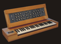
Operation similar to the Mini Moog. The device is already built in a prototype version and works well. At the moment, the printed boards and circuits are optimized and a new operating panel similar to the Minimoog is being constructed. Circuits and layouts will be published here in case of interest and put to discussion for further improvement. See also:
and
https://www.youtube.com/watch?v=LdBCZ-NzvFA&feature=youtu.be
(German short version)
(Detailed English version)
Are you missing the text of all units presented here before?
For a better overview on this page, the complete text which was present here before can now be downloaded as PDF-file from the bottom of this page (See section PCB).
New New New New New New New New New New New New New New
A new, simplified VCO circuit was added under "photographs". Its so simple that it can be mounted on a 16 x 10 cm board with 2 VCOs and 2 exponential converters. More information later.
Please note:
26.feb. 2016 - 21:40: There are another few small corrections now in the sawtooth-section of the new Dual-Expo-Dual-VCO circuit diagram.
I am just busy with testing the new PC-board with its very narrow and dense tracks. Both VCOs on the board now work successfully after the corrections !!!!!
Next test will be with both exponential converters.
Correction: Dual ADSR board:
Attention: In the layout of the board, I discovered still a mistake:
The GND pins of IC1 and IC2 are connected among each other, but not to GND.There is a copper track missing at the lower soldering point of long wire bridge going from GND IC1 in direction IC 4. This empty soldering point has to be connected to Pin 7 of IC4 (GND).
A corrected PCB layout will come soon.
Voltage Controlled Filter (VCF)
The voltage controlled filter (VCF) works with four OTAs. As each one has a transfer function of 6 dB per octave, the complete unit has a resulting transfer function of 24 dB / octave, which is comparable to the Moog-VCF. The OTA-filter-stages are well known in literature – so there’s not much to say. The only important extension is IC11: As we have an even number of stages and as each stage has a phase shifting of 180 degrees, we need an extra phase shifting unit (IC11) in the feedback to get the right phase situation when mixing output and input for increasing Q values.
The Q value (called “Emphasis” at the Minimoog) can be set by P5 which is a potentiometer at the front panel. With P6, the setting of P5 can be limited to a value immediately before filter oscillation.
The circuit around IC10 and T1 unites the input control voltages and transforms the appropriate sum voltage into a control current for the OTAs. The control inputs of the OTAs are connected at the Collector of T1.
At the control inputs, we have to distinguish different voltages which are settable via the control panel:
- Base frequency: This is the filter cutoff frequency which is present when no ADSR function is applied. P4 must be set in a way that the upper limit of the audible range is reached if P1 is set to maximum (turned to the right).
- ADSR: P2 must be set in a way that the upper limit of the audible range is reached if P1 is set to minimum and P0 is set to maximum.
- The tracking potentiometer P3 must be set in combination with the appropriate exponential converter (see below). This connection can be unused for first tests.
- Modulation: Set R1 to a value that the filter frequency is modulated over its whole range when setting the potentiometer for the Filter-Modulation-Amplitude to maximum and P1 to minimum.
The values R1 to R4 are only proposal and must eventually be changed to get the desired results. Lowering the values gets higher amplitudes of the appropriate input channels.
Tracking:
The filter can be operated without using the tracking input. This has the disadvantage that the filter frequency remains constant while playing different keys. If the filter cutoff-frequency is in the middle of the given keyboard range, it is logical that notes played below the cutoff frequency have lower amplitudes than notes higher than the cutoff frequency.
If you use the tracking option, the cutoff frequency will follow the pitch played on your keyboard, which gives a better sound characteristic in many cases.
When using the tracking function, you have to build a third version of your exponential converter.
All filter control voltages like tracking, modulation, base frequency and ADSR have to be connected to the input of the exponential converter – including the keyboard output voltage (KOV). The output voltage of the exponential converter then has to be connected to one of the resistors between R1 and R4, while all other inputs must stay open.
Adjustment of expo converter
As I didn’t yet carry out measurements concerning the voltage-frequency ratio of the VCF, you have to adjust the converter by hearing in the same way that you adjusted the VCOs. That’s a little difficult because the filter does not oscillate. Juts use a ramp or pulse signal with many harmonics and a high Q-value, deactivate the ADSR-function and put P1 in a middle range. Now try to play different notes on the keyboard and see if the filtered harmonics will follow.
To find out a better method, we at first have to find out if the VCF is really linear in its relation between input voltage and cutoff-frequency, and if so, how many volts do we need at the input to shift the filter about a certain frequency.
Layout
At the moment, there exists a layout of the VCF with an additional VCA. At this layout, the trimmers at the control input are not present. At the moment, I am busy to make a better layout including an exponential converter for the filter. The existing layout will be published nevertheless after the description and the diagram of the VCA (coming very, very soon).
Voltage Controlled Amplifier (VCA)
Image 8 shows the diagram of the VCA. The circuit is very simple and represents a kind of simplified Formant-VCO: Everything which is not absolutely necessary, was omitted. Nevertheless it works satisfiying. In the VCA the same OTA is used as in the VCF. The amplitude between signal input and signal output is controlled from zero to maximum via the current at pin 5. IC1 works as voltage-current converter and has the same function as in the VCF circuit. There is only one control-input for the ADSR signal. With P1 the maximum amplitude for the ADSR signal can be set. If the amplitude is too high, the ADSR signal is clipped. If its too low, the stage is not driven to its maximum which results in dynamical loss.
P2 must be set in a way that the signal just gets audible if you would keep on turning it further (but don't do it) with no ADRS signal at the input.
For amplitude modulation purposes, additional inputs of the same kind as the existing ones can be added.
Do'nt forget that the pre resistors R1 and R2 are only recommended values that must perhaps be replaced by higher values due to voltage and component tolerances. The best way is to find out the right values by yourself. The same goes for the VCF by the way.
As you can see in the wiring scheme, its recommended to build up two of these simple VCAs and set the mixing stage after the VCOs. This will result in better dynamic abilities as the VCAs have a low background noise. Both VCAs then can be contolled by the same ADSR unit. But be careful: Until now this is only theory because I didn't yet try it (but I will soon). Maybe there could be some unforeseen complications.
The next and last module will be a noise generator. Im am still looking for a simple and reliable circuit and have to do some experiments.
In addition I will design new PCB-Layout combinations for VCF, VCA, Mixer, Noise Generator and ADSR. There are a lot of possibilities to combine them in a practical way and I didn't yet make up my mind.
It may be possible that I will carry out some changes in the diagrams time by time to improve the circuits. This will be published by an appropriate comment.
At the moment, the prototype with the new boards and the large operating panel is built up partly (both VCOs work and can be controlled in frequency, modulation degree and waveform). The whole device is under test now.
Keyboard
Still one word to the Keyboard and the Sample and Hold unit: Its especially designed for the A-100 CGK (CV/Gate) keyboard of the German company Doepfer, a specialist for synthesizer components. This microcontroller matrix-keyboard has different outputs (e.g. MIDI). I use the analog voltage output (1 V/ octave) and the Gate output (5 V if a key is pressed, 0 V if the key is released). If a key is pressed before the last key was released, the Gate voltage is interrupted in the range of microseconds to retrigger the Sample and Hold stage. The keyboard can also be set to a different behavior concerning different keypress-combinations via some switches.
Wiring schemes
Under "photos" I added two wiring schemes showing how to connect the modules presented until now. The boards connected as shown in the first diagram are the heart of the sound creating unit of the synthesizer. The rest (ADSR, VCA and VCF) belong to the sound modifying units. The red marked switches and potentiometers in the first scheme are part of the operating panel elements.
When printing the Layout
Please format to 16 x 10 cm to achieve the correct measures.
Always use a laser printer and no inkjekt to print the layout. Only use special transparent sheets for laser printers.
The layout is shown mirrored (component view). Why? Most printers are constructed in a way that the printed side of the transparent sheet is on the copper side of the board when the image is in the right position and drawn in the way we see it here.
The printed side must ALWAYS be face to face with the copper layer! This has to be the case to avoid blurred copper patterns on the ready board due to the thickness of the transparent sheet.
Use only laser printers which guarantee a dark black structure of the pattern.
Discussion (6 commentaire(s))