
thermal stability of the quiescent current in audio amplifiers
In the present article offered new way providing thermal stability of the quiescent current in audio amplifiers in the Class AB mode .
In the present article offered new way providing thermal stability of the quiescent current in audio amplifiers in the Class AB mode .
Traditionally, to provide the required amount of quiescent current for the output power transistors of audio amplifiers operating in Сlass AB mode, bias circuits are utilized based on diodes, transistors, or a combination thereof, utilizing a decrease of voltage at an open p-n junction with an increase of its temperature when a fixed current flows through it. This dependence is known as -2 mV per degree C. Typically these devices are located on the same heat sink as the output transistors, thereby providing negative thermal feedback, ensuring the necessary quiescent current for the output transistors in AB mode.
The ON Semiconductor has released a line of power transistors specifically designed for audio amplifiers that incorporate a diode directly on the transistor chip, called the "Thermal Track" series, which allows, with high precision and design simplicity, ensuring temperature stability of the output stage of an audio amplifier operating in Class AB mode.
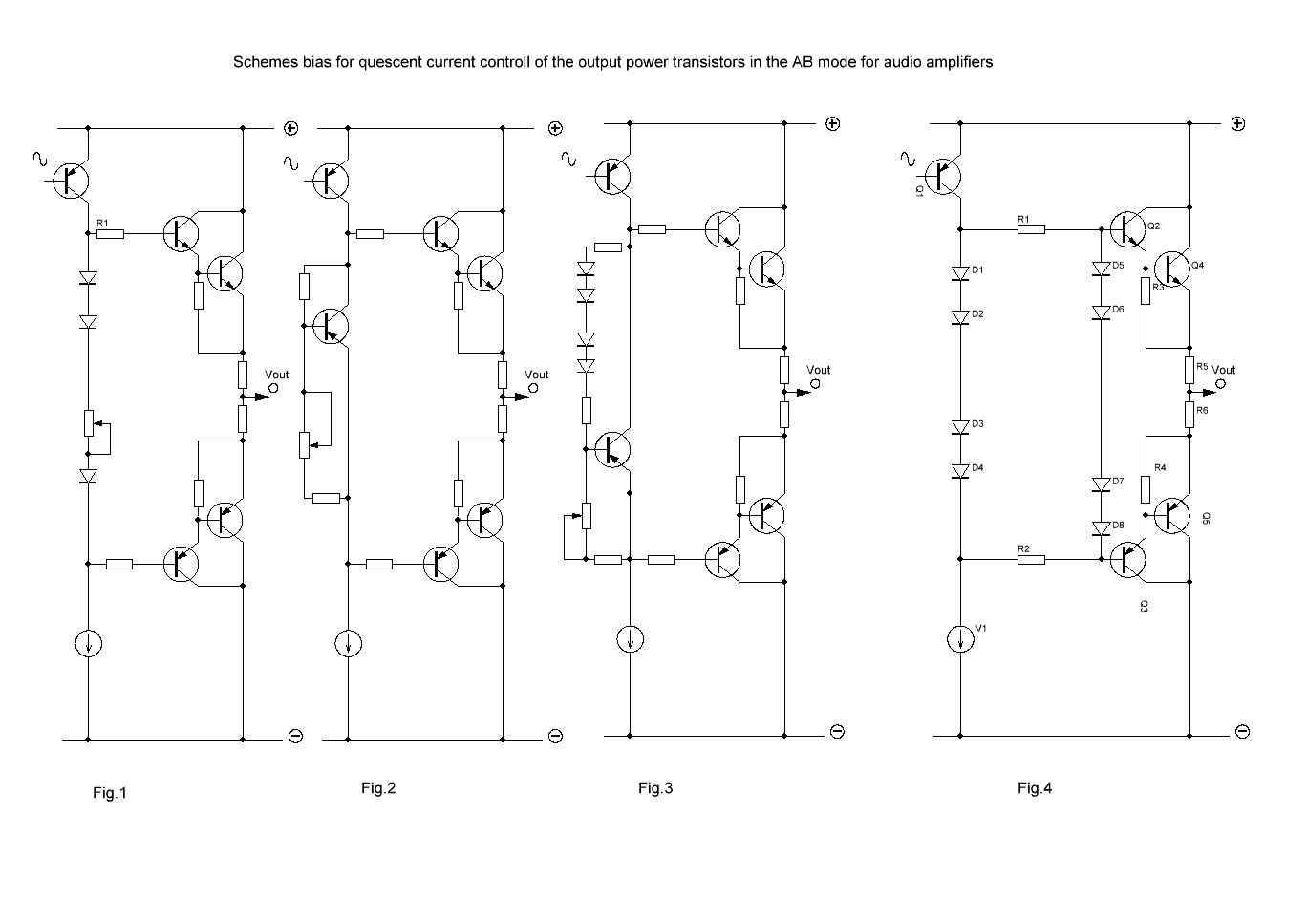
On Fig. 1 – Fig. 3 are shown classic bias circuits for output transistors operating in Class AB mode. In all of these cases it is necessary to match the quiescent current of the output stage transistors using a potentiometer for each individual amplifier channel, as well as when it is necessary to change transistors.
In the present article offered a bias circuit for the output stage of an audio amplifier operating in Class AB mode that offers increased temperature stability of the output stage, small dependent of variations in the parameters of the output power transistors used.
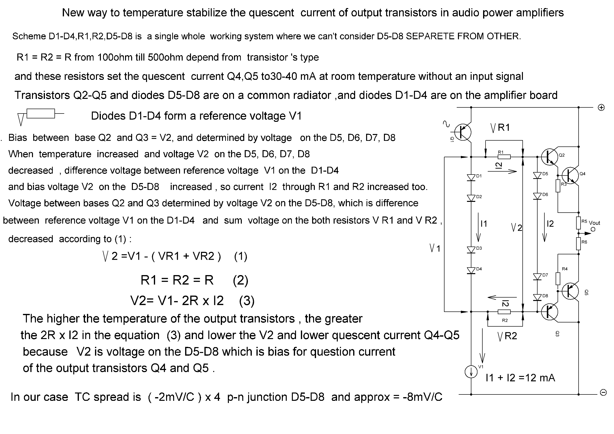
Fig. 4 is a circuit diagram displaying principle of operation of the present bias circuit .
The present bias circuit consists of diodes D1, D2, D3, D4, D5, D6, D7, D8 and resistors R1 and R2.
The diodes D1, D2, D3 and D4 are connected in series and inserted into fixed by the current's generator V1 establishing a reference potential for biasing the output stage of the power amplifier, operating in Class AB mode.
To the reference potential, formed by the voltage drop across the diodes D1, D2, D3, D4, through resistors R1 and R2 connected a temperature dependent auto-bias circuit, consisting of the diodes D5, D6, D7, D8, between bases of the transistors Q2 and Q3.
The resistor R1 is connected between anode of the diode D1 and base of the transistor Q2 and anode of the diode D5. The resistor R2 is connected between cathode of the diode D4 and base of the transistor Q3 and cathode of the diode D8. The diodes D5, D6, D7, D8 are connected in series with each other and inserted between bases of the transistors Q2 and Q3.
The transistors of the powerful output stage Q2, Q4 and Q3, Q5 are connected according to the Darlington circuit and placed on a common heat sink to dissipate the heat of these output transistors. Resistors R5 and R6 form circuit of the thermal negative feedback .
The diodes D5 and D8 are incorporated directly on the chips of the output transistors Q4 and Q5, respectively. The diodes D6 and D7 are placed onto the same heat sink as the output transistors establishing thermal connection with the heat sink. It would be ideal if both these D6 and D7 were located on the crystals of the final transistors Q4 and Q5. Same case is possibly when using two transistors in pair in the output stage , but it is expensive and no need in the case of the power till 200 Wt .
In the absence of an amplified signal and at a room temperature of the heat sink of the output transistors, the resistors R1 and R2 of the equal value set the quiescent current of the output transistors Q4 and Q5 through the emitter resistors R5 and R6 to around 30 mA – 40 mA. Moreover, the current flowing through the circuit R1, D5, D6, D7, D8, R2, is determined by the voltage difference between the reference voltage across the diodes D1, D2, D3, D4 and the bias voltage across the bases of the transistors Q2 and Q3 – voltage across the diodes D5, D6, D7, D8.
When the signal is amplified, the temperature at the output transistors increases and the quiescent current of the output transistors Q4 and Q5 , voltage on the R5 and R6 increased and decreased voltage between bases and emitters output transistors , also the bias voltage on diodes D5, D6, D7, D8 between the bases of Q2 and Q3 decreases with increasing temperature due to the properties of the p-n junction (Fig. 5) .
This method foundation on the increasing voltage on the resistor if current through this resistor increasing in accordance with Ohm’s Low. Bias between base Q2 and Q3 determined by voltage on the D5, D6, D7, D8 . When temperature increased and voltage on the D5, D6, D7, D8 decreased , difference voltage between reference potential D1-D4 and bias voltage D5-D8 increased so current through R1 and R2 increased too. In same case voltage between bases Q2 and Q3 determined by voltage on the D5-D8 which is difference between reference voltage on the D1-D4 and sum voltage on the both resistors R1 and R2.
The greater the voltage difference between D1-D4 and D5-D8, the greater the current through resistors R1 and R2 and the lower the bias voltage between the bases of Q2-Q3 and, consequently, the lower the quiescent current of the output transistors Q4-Q5. Increasing the current along the R1, D5-D8, R2 circuit leads to a decrease in the current through D1-D4, slightly reducing the voltage on them.
This processes provide temperature stabilization of the quiescent current of the output transistors.
The values of these resistors R1 and R2 are in the range from 100 ohms to 500 ohms depending on the types of output transistors used and are selected for a specific type of transistors based on the value of the quiescent current of the output transistors about 30-40 mA at a room temperature.
Let's take a closer look at the mechanism of operation of the auto-bias circuit:
The reason for the decrease in the bias voltage between bases of the transistors Q2 and Q3 is the increase in current through resistors R1 and R2 due to the following two properties of a p-n junction when operating at elevated temperatures:
The first property: increase of voltage difference between the reference potential across the diodes D1, D2, D3, D4 and the bias voltage across the diodes D5, D6, D7, D8 due to decrease in the forward voltage at p-n junctions of the diodes D5, D6, D7, D8 at the rate of -2 mV per 1 degree C.
The second property: additional increase in voltage across resistors R1 and R2 due to an increase in the forward current through p-n junctions of the diodes D5, D6, D7, D8 in accordance with the current-voltage characteristic of a diode operating under conditions of increasing temperature (Fig. 5), leading to even greater decrease in voltage across the diodes D5, D6, D7, D8 when combined with the first property.
In turn, the current through the diodes D1-D4 decreases due to the increase in the current through the circuit R1, D5-D6, R2, since the total current through these circuits is determined by the stable current generator V1. In this case, as a consequence, the voltage on the diodes D1-D4 decreases and the reference bias voltage of the output transistors Q4-Q5 decreases and, consequently, the total bias for the output transistors Q4-Q5 decreases. In this case, the efficiency of the thermal negative feedback through the emitter resistors R4, R5 of the output transistors Q4, Q5 also increases.
Taking advantage of properties of a p-n junction, i.e., : decrease of forward voltage across a diode with decrease forward current , decrease of forward voltage across a diode with increase of temperature and increase of forward current through a diode with increase of temperature, for temperature stabilization of a powerful output stage of an audio amplifier operating in Class AB mode, in contrast to the traditional use for this purpose only the decrease of forward voltage across a diode with increase of temperature, allows achieving significantly higher magnitude of negative thermal feedback, which make thermal stability output transistors small dependent from of variations in the parameters on their operation in Class AB mode.
Karnaushenko Sergiy
Kyiv

Discussion (0 commentaire(s))