
140571 Active 3way crossover for speaker system
Designed by A. Rosenkränzer This 3-way filter is originally designed in conjunction with the power amplifier we published earlier (130007-1).
Designed by A. Rosenkränzer
This 3-way filter is originally designed in conjunction with the power amplifier we published earlier (130007-1). But the filter can also be used in combination with any other power amplifier to create an active speaker system (Figure 1).
The circuit has a differential input and can be connected by way of standard XLR cables (see Schematic Figure 2). The differential input signal is converted into a single ended one before it goes to the filter sections. A fourth order Sallen-Key low pass filter is used for the bass signal and a fourth order Sallen-Key high pass filter for the tweeter signal. For the mid-range frequencies a combination of a fourth order Sallen-Key low pass and high pass filter is used. The signals of the filter sections are connected to three potentiometers and each buffered to create an adjustable signal with low impedance for the relating power amplifier. There’s an extra option in the bass buffer for a bass boost or simple amplitude correction (R46/R47/C27..C30). In case a 2-way system is used the mid filters are not necessary and the cut-off frequencies of the tweeter and bass signal should of course be calculated accordingly. Instead of fourth order filtering third or second order filtering is also possible by leaving components out and bypassing other ones. About the different topologies a lot of information can be found on the internet, like calculating tools for the filters. As an example the values of the filter components in the schematic are calculated for a 4th order (24 dB/octave) Linkwitz-Riley filter with crossover frequencies of 800 Hz and 5 kHz. Summing the three outputs will produce a perfect straight frequency response (in theory). Component tolerances will degrade the performance but above all speakers will have the biggest influence on the final frequency response.
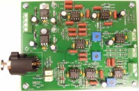
Two voltage regulators are present to produce a symmetrical power supply (+/-12 V). Two leds indicate the supply voltages are present. Diodes D5 and D6 are put in series with the regulators as a polarity protection. Gain in the differential amplifier at the input (IC1) is optional. R7 is not mounted. Gain is also possible in the output buffers, but is not implemented either. R21, R36 and R47 are not mounted. The filters have unity gain in their pass band. The signal arrives through K1.Pin 2 is +, pin 3 is - and pin 1 is ground. A special connecter is used for K1 combining XLR and ¼” jack (6.35 mm). R1 and R2 connect the XLR and R49 and R50 connect the jack. For standard home use we recommend the XLR and leave R49/R50 open. We mounted R49/R50 for testing purposes. In case of disturbances the case of K1 can be connected to ground by R14 and/or C1 (experiment what’s best). A similar story applies to C4, C5 and C6 . These capacitors suppress HF noise (C4 in combination with R1/R2 or R49/R50) and can be used if necessary. C5 and C6 can also simply be used to filter out frequencies above the audio spectrum. D1..D4 protect the input stage against extreme voltages. R8..R13 have identical values and should be in the kΩ range. Lower value will increase distortion and higher values will increase noise. Difference amplifier IC2A drives the filter stages. Filter capacitors in the high pass filters have equal values (E-12 used, E-24 can be difficult to get). Resistors in E-96 can be accurate enough (like 2.26 instead of 2.25) or E-24 resistors are paralleled where necessary. 4th order Linkwitz-Riley are two 2nd order Butterworth in series. The crossover frequencies are at the resulting -6 dB cut-off frequency. That’s why the filter components in two successive filters have identical values. The 100 Ω resistor in the output of the buffers prevent oscillations should the capacitive load be to high (from cables). In the low pass filters two capacitors are paralleled to get the exact double value of the other capacitor. The output stage of the mid-range section is identical to the one of the tweeter output (we called this output high, less characters on the PCB). The bass filter is connected to IC2A by R40. In this implementation of the Linkwitz-Riley filter R39 should not be mounted. The output stage for bass can also be used to create a bass-boost (R47, C27..C30). Usually high and mid-range speakers have a higher output level than bass speakers, so gain is probably not necessary here. To have the bass output stage amplify short the position for C40 or C41 on the PCB and place a resistor for R47. The gain of buffer IC7B is then 1 + R46/R47. We used the good old NE5532A for all opamps. For the resistors we recommend the use of metal film resistors, and metallized film capacitors for the filter capacitors. The decoupling capacitors (C31..C44) can be ceramic ones. If anyone thinks film capacitors here will improve sound quality, these can also be used. For best performance the top layer of the PCB is one big ground plane. This can reduce the problem with ground loops. Also the copper plane also acts as a small heatsink for the regulators. The metal tab of the positive regulator 7812 can be fastened directly to the PCB. The negative regulator should be an insulated one, the version with a metal tab has it connected to the input voltage. In many active speaker systems the power supply for the power amplifiers is one and the same. Input ground of the power amplifier is generally connected to ground of the power supply. If ther’s one power supply then the power ground connections of the amplifiers are connected to each other and the input grounds are connected by the filter, forming a big ground loop. Good practice in this case is keeping wring as short as possible. In principle, if the power supply voltage is not to high (< 25 V), the power supply for the filters (input of the 12 V regulators) can be derived from the power supply of the power amplifiers. But this would make the ground loop(s) even worse. Best is to use a separate power supply for the filter (see Figure 3). The photo shows our first prototype.
Some measurements (all input and output stages unity gain, 1 Vrms input signal)
THD+N, B = 22 kHz
low output 0.0003 % (100Hz)
mid output 0.0003 % (2 kHz)
high output 0.0005 % (7 kHz)
Current consumption about ±56 mA
We also recorded some plots with our Audio Precision Analyzer
Plot A (Amplitude_P1-P2-P3_max_1.emf) shows the amplitude of the three filter outputs as a function of frequency. Clearly visible are the two crossover frequencies at -6 dB at 800 Hz and 5 kHz.
Plot B (Amplitude_P1-P2-P3_cal_sum_1.emf) shows the sum of the three outputs as a function of frequency. This was done by connecting three 10 kΩ resistors in the outputs together. The upper curve is measured with all three potentiometers at maximum. The deviation of more than 0.6 dB from a perfect straight line is caused by component tolerances but also the fact that the filters capacitors have an ESR and the two crossover frequencies are influencing each other. The lower curve is measure after correcting the potentiometers for bass and treble to produce a lower deviation. Amplitude of the bass output was lowered by approximately 0.4 dB and treble by approximately 0.2 dB. The devation is now less than 0.4 dB.
Just for fun: we also measured the each output of the four mid filters sections (Plot C, Amplitude_four_mid_sections_1.emf).
Plots D, E and F show THD+N in the low, mid and high outputs (THD+N_LOW_1.emf, THD+N_MID_1.emf and THD+N_HIGH_1.emf). De frequency range of each plot was limited to the a specific bandwidth for each filter. The apparent increase in distortion plus noise outside the crossover frequencies is mainly noise due to the fact that amplitude is decreasing rapidly. All three plots were measured with a larger bandwidth of 80 kHz, given the higher frequency range for the HIGH output measurement. This gives a slight increase in noise.
Bill of materials
Resistor (metal film, 0W25, 1 %, 250 V)
R1,R2,R5,R6,R49,R50 = 1 kΩ
R3,R4,R32,R33 = 100 kΩ
R7 = not mounted
R8-R13,R22,R29,R31,R37,R39-R43,R46 = 3.0 kΩ
R19,R51 = 3.3 kΩ
R14 = not mounted
R15,R17 = 4.7 kΩ
R16,R18,R24,R25,R26,R27 = 2.26 kΩ
R20,R35,R45 = 10 kΩ
R21,R36,R47 = not mounted
R23,R38,R48 = 100 Ω
R28,R30 = 6.2 kΩ
R34,R44 = 180 kΩ
P1,P2,P3 = 20 kΩ
Capacitor
C1 = not mounted
C2,C3 = 1 µF, 63 V, 5 %, PET, lead spacing 2.5/5mm
C4,C5,C6 = not mounted
C7-C16 = 10 nF, 250 V, 5 %, PET, lead spacing 5/7.5 mm
C17-C26 = 47 nF, 100 V, 5 %, PET, lead spacing 5/7.5 mm
C27-C30 = not mounted
C31-C44,C52,C53 = 100 nF, 50 V, 10 %, X7R, lead spacing 5.08
C45-C51,C54,C55 = 22 µF, 63 V, 20 %, diam.7mm max., lead spacing 2.5mm
Semiconductor
D1-D4 = 1N4148, 100 V, 200 mA
D5,D6 = 1N4007, 1000 V, 1 A
LED1,LED2 = LED, green, 3 mm
IC1-IC7 = NE5532AP
IC8 = MC7812, 12 V, 1 A
IC9 = L7912CP (Insulated, full plastic case)
Other
K1 = 3way XLR / 1/4" Jack, Socket, R/A, NCJ6FA-H Neutrik
K2,K3,K4 = Terminal block 5.08 mm, 2way, 630 V
K5 = Terminal block 5.08 mm, 4way, 630 V (or 2 x 2way)
Misc.
PCB 140571-1 v1.1
Want to build a project?
Bring your design to life with the Elektor PCB Service, powered by Eurocircuits. Upload the project files and order professionally manufactured PCBs or assembled boards through a proven European production platform.
Supporting KiCad, Eagle, Gerber, and ODB++ formats, the service is suitable for everything from prototypes and validation builds to series production and volume manufacturing.
Made in Europe. Fast. Reliable. Professional.
Discussion (2 commentaire(s))