Simple audio power amplifier
Download the Elektor article below.
It all started with the Measurement Filter for Class D (100540-1) published in issue 415, July/August 2011. It was designed to handle large output signals, up to 70 V (RMS!). We never came around to really test the filter at the highest levels. A completely discrete high voltage amplifier design was started with 23 high voltage transistors (MJE340, MJE350, MPSA42 and MPSA92) working with a split power supply of +/- 110 V. This design got a bit out of hand. Even a PCB for a first prototype was designed but then one thinks ‘all this just to test a filter?’ The amplifier should be able to deliver a signal with extreme low distortion up to 20 kHz at 70 V. The impedance of the filter is 1 kΩ minimal, so 100 mA peak output current is necessary (more would be preferable). Looking for an alternative like an integrated circuit that can handle these high output voltages we came across the LME49811 from Texas Instruments. The title of the datasheet ‘Audio Power Amplifier Series High Fidelity 200 Volt Power Amplifier Input Stage with Shutdown’ was inviting to have a closer look. The specifications are excellent. Although one thing is not entirely clear from the datasheet. Are the measurements made according to the Test Circuit which omits the entire output stage? No examples are mentioned for the output stage. Another strange thing is the missing of the bottom layer of the Demonstration Board Layout which is visible in an older version of National Semiconductor from 2008. But we still went ahead and designed an amplifier with this component.
One of the most important properties for the possible candidates for the power transistors (T4/T5) in the output stage is a very wide safe operating area. Eventually we found some very nice ones from Semelab Limited, the MG6330-R (NPN) and its complementary MG9410-R. At 200 V across collector and emitter more than 600 mA of collector current may flow. This will be the case when the amplifier is driven to maximum output swing with no load. A wide class A setting in an class AB output configuration is now possible. The DC current gain versus collector current is almost constant up to several amperes (a little less for the PNP version) contributing to a linear output stage. Similar demands are valid for the drivers (T2/T3) of the power transistors. The MJE15032 (NPN) and MJE15033 (PNP) can handle 250 V maximum and the DC current gain is also reasonably constant with changing collector current. Both drivers and power transistors have high transition frequencies: 30 MHz for the MJEs, 60 MHz for the MG6330-R and 35 MHz for MG9410-R. For the quiescent current control an ordinary BD139 is used.
At first the design was meant for our July/August edition. But then one of our editors asked ‘Who needs this kind of amplifier?’ Can it not be used as an ordinary audio power amplifier? Yes of course it can, but not without a few additions and modifications. At a lower power supply voltage the output stage is able to deliver a lot of power to a speaker! Quiescent current can be 3 A at 120 V across. To keep it a simple amplifier we assume the amplifier is going to be connected to speakers with standard impedances from 4 Ω to 8 Ω, where 3 Ω is considered to be the lowest allowable impedance. At a power supply of +/-60 V and a 3 Ω load the output transistors will be driven outside their DC safe operating area but stay well within the 100 ms curve. For that reason we advise to use a 2 x 40 V transformer. We used a cheap 500 W version with a regulation that could be better. In practice this means a higher supply voltage without load or when little output power is delivered. With a lower mains voltage (224 instead of 230!) we measured around +/-56.8 V DC in our test setup. As a precaution a Zobel network is added (R13/C5). This network ensures the amplifiers stability in case there is no load. It also helps when the load is highly inductive. Inductor L1 is an extra protection against capacitive loads. Resistor R12 dampens any ringing or resonance that may occur. On the PCB R12 is placed inside L1, this is only done to save space.
Apart from the output stage the LME49811 only needs a few components to complete the amplifier. With the value chosen for the feedback resistor, should one of the power supply voltage (60 V max.) be present at the output, the maximum dissipation will not be more than the maximum specified by its manufacturer. In our case that’s a little under 0.25 W. This results in 15 kΩ for R4. To give the amplifier the correct gain we take into account a maximum output swing of 5 V below the power supply voltage. At 60 V DC this means 55 V peak. Over the past years at Elektor we dimension our amplifiers to deliver their maximum undistorted output power (THD+N = 0.1 %) at 1 V input level. Any modern day preamplifier is able to supply this level. In our case the gain is exactly R4/R3, taking R1 and R2 into account. This means an E-12 value of 390 Ω for R3 (15k/(55/Ö2)). To keep common mode suppression of the input stage of the LME49811optimal the impedance of R1//R2 should be the same as R3//R4. So the values of R1 and R2 are the same as R3 and R4 respectively. The input impedance is approximately 15 kΩ which is also no problem for preamplifiers. The low cut off frequency is determined by C1, in our case theoretically 2.2 Hz. C2 limits the bandwidth of the input signal to suppress HF noise and limit too fast input signals. This will partially reduce slew rate of the amplifier. This is the case when for instance at the input a perfect rectangular signal is present. For compensation only a single capacitor is needed (C3). To make experimenting easy we used a trimmer with PTFE as a dielectric, which is also an excellent choice for audio. The PCB is also suitable for silvered mica capacitors with a lead spacing of 5.9 mm. While testing we noticed the value of C3 can be much less than 30 pF. Adjusting the trimmer to the lowest level, the amplifier remained stable. But we noticed no improvement of measuring results when the capacitor was adjusted below 1/3 of its maximum value. So set it at 1/3 (approximately 18 pF). To avoid any DC voltage at the output we added a DC servo (IC2). It compares the output voltage with ground and corrects the input of the LME49811 (pin 4) with a very small current. The correction is done at the non-inverting input because of the higher impedance of the resistors. R2 is 15 kΩ and at pin 5 the impedance is only 380 Ω (R3//R4). The small current compensates any input offset of IC1 and bias current of pin 4. The control speed is a few tens of a second. That’s why the output relay takes a little longer to activate. The opamp used is a OPA177 and has excellent DC specification. Its own bias current and offset are maximally 2.8 nA and 60 µV. So the largest offset voltage at the output of the power amplifier is caused by the bias current of IC2 through R14. Worst would be an offset of 0.6 mV. When our prototype was stabilized (no output signal) the output voltage was around 0.2 mV only.
Let’s hope the amplifier will never fail, but any electronic circuit will eventually stop working. The junction temperature of the audio power transistors is often driven above 70 °C and that will reduce the life span of the semiconductors. Our experience is failing semiconductor usually becomes a short circuit. If no fuse is blown this means a DC voltage at the output of the amplifier. A DC protection is something no audio power amplifier should go without. After power-up the amplifier needs a few seconds to settle. Like most power amplifiers the speaker is connected to the output by way of a relay. Three conditions must be met before the relay will activate. No DC voltage must be present at the output of the amplifier. Of course the power supplies must be present. In our case the positive power supply is used to power the relay. The negative power supply is not monitored. The last one is the presence of the secondary transformer voltages. If these are not present the relay is immediately deactivated to prevent a DC level over the speakers before it will occur. To prevent a ground loop an optocoupler. D3, D4 and C14 rectify the transformers voltage to a DC level. R19 makes sure, should the mains transformer get switch of or its fuse blown, the voltage over de led inside the optocoupler decreases rapidly to a level at which the opto transistor is no longer active. This in turn will activate T6. Capacitor C16 is then discharged and this in turn will deactivate the relay driver stage. The time constant of C16 and R25//R26 determines the time it takes to activate the relay when the amplifier is turned on (in practice one and half times, so 6 seconds).
The relay is a 48 V version, but the power supply voltage is about 56 V. To limit the voltage over the relay only a small resistor is needed in series with the coil. At 48 V the coil of relay needs only a few mA’s to activate, 8.7 mA to be precise. At 56 V a resistor of 1 kΩ/0.25 W will do. The tolerance of the energizing voltage of a relay is rather large. So even if the supply voltage drops the relay will stay energized. The release voltage is a lot lower than the operate voltage. The release voltage of the relay we used (RT314048) is 10 % of its nominal voltage, so 4.8 V. The operate voltage is 70% of its nominal value, so 33.6 V. If the 48 V relay is difficult to get also a 24 V relay can be used. The energizing current is almost double as high and the dissipation of the series resistor thus a lot higher. The coil resistance of a RT314024 relay is 1440 Ω. In this case a 2 kΩ resistor will have to be used, 2.2 kΩ will also do. The dissipation will be a little over 0.5 W and a 1 W resistor is needed. While designing the PCB we already gave R29 a big enough footprint. Should another manufacturer’s relay be used, the value of R29 can be different of course. In all this the voltage drop of about 1 V across T10 is being neglected. The current through led D6 is also being neglected. With a 48 V relay this current is a mere 0.35 mA. The protection circuit is calculated for the high voltage of 56 V. The operating voltage of the LME49811 ranges from +/-20 V to +/- 100 V. At a lower supply voltage some resistors have to be changed. This is also true for the feedback resistors, when the input sensitivity should remain the same. The gain should be lower at lower supply voltages. The minimum gain of the LME49811 is 20 (26 dB). So in our view the gain at a supply voltage of +/-20V this gain would give a too high sensitivity. The DC protection is basically just two transistors and a low pass filter. The time constant of 3.3 seconds of RC network R23/C15 is maybe a bit long but, the higher the DC voltage the faster T7 or T8 will discharge C16. If a positive DC offset is present at the output greater than 0.55 V the C16 will be discharged enough by T8 to deactivate the relay. If the output is negative T7 will discharge C16. Because the negative current through R23 is directly responsible for discharging C16 the sensitivity is less than with a positive offset.
The decoupling of the power supply is done by way of large electrolytic capacitors with low ESR. These were originally meant as smoothing capacitors in the high voltage amplifier design, so no external ones had to be used. For an audio power amplifier it is critical that the power supply lines leading to the PCB don’t produce any interfering magnetic fields that can increase distortion by inducing currents in feedback loops and other parts of the amplifier. One way to suppress this unwanted effect is tying the three power supply lines close together and decouple the power lines as close as possible at the power stage. On the PCB the power supply tracks have single rectified currents flowing, because of the class AB output stage. By trying to keep the corresponding positive and negative tracks as close as possible together the produced magnetic field is almost sinusoidal and causes les distortion. On a double sided PCB these tracks can be on opposite sides. These design considerations are important for power amplifiers with very low distortion figures. Also a star ground is a must, to be found at C5. Here input ground, feedback, Zobel network, loudspeaker ground and power supply ground come together. So the PCB is specifically designed for a mono amplifier. For a stereo amplifier simply build two.
The opamp for the DC correction has its own +/-15 V power supply, derived from the main supply by way two resistors, two zener diodes and decoupling capacitors (R17/R18/D1/D2/C12/C13). In case a lower power supply voltage is used the value of R17 and R18 has to be reduced. Also take into account that from the positive 15 V the enable current (R5) for IC1 is taken. This current is 1.47 mA. The voltage at pin 1 of IC is in our case 2.92 V (a value not to be found in the datasheet). In principle the biasing of de +15 V is maybe to low but it is sufficient. The supply current of the OPA177 is 1.3 mA and the enable current is 1.47 mA. Together this is more or less the same as R17 delivers (2.78 mA at 56.8 V). The main supply voltage can drop because of excessive output power. At 233 W sine-wave power to a 4 Ω load the power supply was only 48.9 V. In this case the current through R17 is only 2.26 mA. But the enable current of IC1 may be as low as 1 mA and the supply voltage of IC2 is much higher than needed. The most important function of D1 and D2 is to make sure the power supply voltage of IC2 is never higher than +/-15 V. In our prototype the output of IC2 was not even 1.1 V. Power supply rejection of IC2 and the additional filtering by C11 make sure that the quality of the amplifier is never influenced. The typical bias current of the LME49811 is 100 nA, the maximum is not specified. We measured less than 37 nA. Additionally the maximum input offset is 3 mV. So in worst case the offset correction needs to compensate 4.5 mV of total input offset voltage. For IC2 this means a maximum output voltage of 6 V ((4.5mV/15kΩ)*20MΩ). Should a higher voltage than 6 V occur something is not in proper working order.
The maximum power dissipation of IC1 is almost proportional with its power supply, although the
power supply current increases slightly with increasing power supply voltage. From the datasheet we derived that at +/-60 V the maximum supply current is 18 mA. This is independent of any input signal. So
the power dissipation of IC1 is in our case a little over 2 W (2.16 W at 120 V total). As a heat sink we used a simple 2 mm thick aluminum plate. Calculating the thermal resistance is not that difficult. De datasheet states the thermal resistance from junction to case is 0.4 °C/W and using a thermal compound tha thermal resistance from case to heat sink approximately 0.2 °C/W. Let’s make that a total of 0.8 °C/W, just to be safe. Total dissipation is about 2.16 W. If we want the driver to have a long life we advise to keep the junction below 70 °C. In an enclosure the ambient temperature will be higher than the surrounding room temperature, let’s say 40 °C. That makes the necessary resistance from junction to ambient 30 °C/2.16 W = 13.8 °C/W or lower. The thermal resistance of the heat sink should be 13 °C/W. If we search the internet (but not too long) for a formula or graph to find out how big the aluminum plate should be we came across 2 formulas and a graph. The first formula 500/A (A in cm2, both sides) resulted in a necessary surface of 19 cm2 (size). The second formula 50/ÖA (A in cm2) gives a surface of 14.8 cm2 which is substantially smaller. We had to extrapolate the graph. For a plate of 2 mm thick the curve ends at a surface of 30 cm2 (Rth = 7.9 °C/W). Extrapolation to 20 cm2 gives a thermal resistance of 9.5 °C/W. Our plate of 2.5 by 8 cm will be sufficient, no matter what solution to believe. We measured the temperature of the heat sink. At a room temperature of 20 °C the heat sink became 49 °C. With a power dissipation of 2.16 W this means our heat sink effectively has a thermal resistance of 13.5 °C/W. Components like L1 and C8/C9 limit convection somewhat and thus the thermal resistance of the plate will be higher. The PCB is designed to give the plate just enough room, from C10 to C8/C9. Mount the plate to IC1 with enough distance from the PCB so it won’t come in contact with R1, R5 and R4. Bend L1 a little from the heat sink. Important: the metal part of the backside of IC1 is connected to the negative supply voltage. If only a thermal compound is used between heat sink and IC there is a big chance the heat sink is also connected to the negative supply voltage, in our prototype it was!
An important part of any power amplifier is the heat sink for the power transistors. How large should it be? This amplifier is able produce a lot of power with only 1 set of power transistors. Usually with this amount of power two pairs are used at least. More transistors in parallel would increase efficiency of the amplifier. Especially at 4 Ω loads the two emitter resistors of 0.2 ohm are responsible for a loss of 5 % alone. Two extra power transistors would increase the size of the PCB and we wanted to keep this a small (the PCB at least) and simple amplifier, but with very good specifications none the less. We found a compromise in a heat sink from Fischer Elektronik. Not exactly small but to ensure no thermal runaway will occur with high output power a very low thermal resistance is necessary. At a height of 100 cm its resistance is 0.7 °C/W. An example: we measured the efficiency of the amplifier with a regulated DC voltage of +/-56.8 V. In a 4 Ω load the amplifier will deliver 299 W at a distortion of 0.1 %. Now the efficiency is 68.5 % and the loss of the amplifier 137 W. Most power will be dissipated in the large heat sink. Without extra measures its temperature wood rise more than 90 °C above ambient if a pure sine-wave signal is used continuously! Also the emitter resistors R10 and R11 (5 W resistors) will be strained to their maximum and when the output is clipping may be even beyond that. But with music the real power will of course be substantially less, in the heat sink and R10 and R11. When testing we use a large tangential blower to avoid damaging the power amplifier.
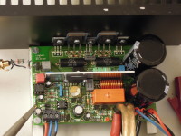
Construction of the amplifier depends for a large part on the enclosure that is going to be used. For testing we attached two metal bars to the heat sink to mount the PCB on. This way no mechanical stress is applied to transistors in the output stage. The PCB should be mounted against the heat sink so the pins of the transistor are as close to their respective pads on the PCB as possible. The pins get a double bend. The first bend should be as close to the transistors packadge as possible. Never bend de legs directly but put a metal plate against the pins to avoid micro fractures in the packadge. These can reduce the lifespan of the transistors. The second bend is where the holes in the pads are. The insulation of the transistor can be placed between transistor and heat sink before locating the exact position for the second bend. But that isn’t too critical except when ceramic insulators are used, they really make a difference. After this is done there will be no thermal stress as well. The transistors are mounted firmly on the heat sink after the PCB is already mounted (don’t forget the insulating pads). Only then the pins of the transistors can be soldered. Most components can be soldered before all of this is done, except for IC1 and the power supply capacitors C8 and C9. They are mounted and soldered after placement of the power transistors is finished. The heat sink of IC1 will be in front of the screws of the transistors of the power stage. Leaving the power supply capacitors to the end will give a clearer view when mounting the power transistors. IC1 is the last component to be mounted at this point (or earlier) the exact placement of the aluminum plate and the holes for the mounting of IC1 can now be determined (2.5 cm high and 8 cm long). As stated earlier, leave enough space between the PCB and the heat sink to avoid contact with parts that are the closest to it. To really rule out a possible short circuit to the heat sink, a fitting insulating pad can be placed in-between IC1 and its heat sink. This doesn’t change the total thermal resistance that much. Mount the aluminum plate onto IC1 before soldering IC1 to the PCB. This will avoid mechanical stress to the pins of IC1. For connecting the speaker and the power supply mounting tabs with two pins are used (faston, 6.3 x 0.8 mm lead spacing 5.08 mm). Most terminal blocks can’t handle currents over 5A or so. Peak currents in the speaker output and power supply can be close to three times as high. The relay used is rated 16 A. A last detail concerns the construction of L1. L1 is made of 13 windings of 1.5 mm (diameter) enamelled copper wire wound on a 7 mm drill. Leave the endings long enough to mount the inductor with a little distance from the PCB. The endings of the inductor should be in line with the center of the inductor. Resistor R12 is then placed inside L1 and its connecting wires bend to correspond with the pads on the PCB. Place the two components simultaneously on the PCB and look if the resistor remains in the center of the inductor and the inductor a little distance from the PCB before soldering the four wire endings.
Before connecting the amplifier directly to the power supply the quiescent current of the output stage needs to be set. We advise as a precaution to put two 47 Ω/5 W power resistors in series with the PCB power supply connections (in plus and minus). Should something be wrong (a short circuit somewhere) chance is the amplifier itself will not be damaged but in worst case the two power resistors will burn out. The use of a regulated power supply would be better but who has access to a dual power supply that can be set to +/- 56 V or so. Before switching on the power supply turn P1 fully counter clockwise. Current consumption in the positive power line should be about 30 mA (with activated output relay). Screw terminal K7 should be connected to the transformer of the power supply. Put an ampere meter in series (with the power resistor) and turn P1 slowly clockwise until the current increases 30 mA, resulting in a reading of 60 mA. This low setting is more than enough. If the temperature of the heat sink rises the quiescent current will also rise slightly but should stay below 90 mA. At high power output the temperature of the junctions of the two power transistors T4 and T5 will rise a lot more than the temperature of the heat sink and thus VBE multiplier T1 will not compensate this fully. Momentarily the quiescent current will rise to several 100 mA, but will fall when power is reduced and the heat sink cools down again. In this the amplifier has a nice extra. You could say the class A setting of the output stage rises with the supplied output power.
Measured performance
Power supply: mains transformer 2 x 40 V/500 VA (Nuvotem 0500P1-2-040), 4 x 10000 µF/100V
Input sensitivity 0.88 V (137 W/8 Ω, THD+N = 0.1 %)
0.91 V (145 W/8 Ω, THD+N = 1 %)
Input impedance 15 kΩ
Sine-wave power 137 W (8 Ω, THD+N = 0.1 %)
145 W (8 Ω, THD+N = 1 %)
220 W (4 Ω, THD+N = 0.1 %)
233 W (4 Ω, THD+N = 1 %)
Peak/Music power 218 W (8 Ω, THD+N = 10 %)
(+/-56.8 V DC power supply) 175 W (8 Ω, THD+N = 1 %)
165 W (8 Ω, THD+N = 0.1 %)
395 W (4 Ω, THD+N = 10 %)
316 W (4 Ω, THD+N = 1 %)
299 W (4 Ω, THD+N = 0.1 %)
Power bandwidth (50 W/8 Ω) 2.1 Hz…125 kHz
Slew rate 26.7 V/µs
Rise time 2.4 µs
Signal to noise ratio >94 dB (B = 22 Hz…22 kHz linear)
(Referred to 1 W/8 Ω) >97 dBA
Harmonic distortion plus noise 0.0033 % (1 kHz, 1 W, 8 Ω)
(B = 80 kHz) 0.0006 % (1 kHz, 50 W, 8 Ω)
0.006 % (20 kHz, 50 W, 8 Ω)
0.0047 % (1 kHz, 1 W, 4 Ω)
0.0009 % (1 kHz, 100 W, 4 Ω)
0.009 % (20 kHz, 100 W, 4 Ω)
Intermodulation distortion 0.002 % (1 W, 8 Ω)
(50 Hz :7kHz = 4 :1) 0.0009 % (50 W, 8 Ω)
0.003 % (1 W, 4 Ω)
0.0026 % (100 W, 4 Ω)
Dynamic IM distortion 0.0033% (1 W, 8 Ω)
(3.15 kHz square wave + 0.0022 % (50 W, 8 Ω)
15 kHz sine wave) 0.0045 % (1 W, 4 Ω)
0.0027 % (100W, 4 Ω)
Damping factor 560 (1 kHz, 8 Ω)
311 (20 kHz, 8 Ω)
DC protection +0.55 V/-0.86 V
DC output offset 0.2 mV (0.6 mV theoretically max.)
Delay output relay 6 s
Efficiency 8 Ω 70 .6 % (THD+N = 0.1 %)
(DC power supply) 72.5 % (THD+N = 1 %)
4 Ω 68.5 % (THD+N = 0.1 %)
70.5 % (THD+N = 1 %)
We also recorded some plots. Pictures tell more than numbers?
Plot A shows measurements of harmonic distortion and noise at output levels 1 W and 50 W into an 8 Ω load with a bandwidth of 80 kHz. The plot at 1 W is mainly noise (THD+N = 0.0034 %). Only at the end towards 20 kHz the distortion slightly rises above noise (THD+N = 0.0052 %). At 50 W (this is 20 V so you can compare it with the datasheet of the LME49811) the noise floor is relatively lower in comparison to the output level. We now can see that distortion is starting earlier, because the noise floor is lower. At 1 W this is masked by the noise. The distortion at 20 kHz is almost similar as the figure at 1 W. A plot at 100 W is not that much different from the plot at 50 W. The figures can differ a bit with temperature and time. At these low levels 0.005 or 0.006 % is not something to worry about, just very good.
Plot B shows distortion plus noise as a function of output level at 1 kHz with an 8 Ω load and a bandwidth of 22 kHz. The reduced bandwidth will show better the onset of increase in distortion. As you can see the distortion of the output signal remains extremely low while the noise floor relatively sinks with the increase of the output level. At 127 W the linear operation ends and the clipping point is reached. Distortion will rise quickly with the increase of the output level now. A THD plus noise of 0.1 % is considered a just level to still speak of a clean and undistorted signal. This is reached at a level of 137 W. If we really overload the amplifier to 10 % distortion the output power is than 174 W. A remark must be made here however. The transformer we used is a cheap 500 VA type (it’s almost impossible to find a smaller transformer with 2 x 40 V) but its regulation is not that good. At 10 % THD the power supply voltage decreased to +/-51.5 V. With increase of output power distortion will rise even more quickly.
Plot C shows a Fourier analysis of a 1 kHz signal at 50 W (20 V) with an 8 Ω load. The residual spectrums of the power supply ripple as well as the harmonics of 1 kHz are at levels that are simply inaudible. The 3rd harmonic is at a level of -113.8 dB. That’s 2 ppm. Do we need to say more…Total harmonic distortion plus noise is at this level 0.0006 % (bandwidth is 80 kHz).
Bill of Materials
Resistor
R1,R3 = 390 Ω, 5%, 0W25
R2,R4,R17,R18,R22,R23,R30 = 15 kΩ, 5 %, 0W25
R5 = 8kΩ2, 5 %, 0W25
R6,R20,R28 = 1kΩ2, 5 %, 0W25
R7 = 220 Ω, 5 %, 0W25
R8,R9 = 100 Ω, 5 %, 0W25
R10,R11 = 0Ω2, 1 %, 5 W, low inductance, Vishay Dale LVR05R2000FE73
R12,R13 = 3Ω9, 5 %, 5 W
R14 = 220 kΩ, 5 %, 0W25
R15,R16 = 10 MΩ, 5 %, 0W25
R19 = 27 kΩ, 5 %, 0W25
R21 = 470 kΩ, 5 %, 0W25
R24 = 1 MΩ, 5 %, 0W25
R25,R26 = 820 kΩ, 5 %, 0W25
R27 = 68 kΩ, 5 %, 0W25
R29 = 1 kΩ, 5 %, 0W25
P1 = 470 Ω, 20 %, 0W15, trimmer, top adjust
Capacitor
C1 = 4µ7, 10 %, 63 V, MKT, lead spacing 5/7.5 mm
C2 = 1 nF, 10 %, 400 V, MKT, lead spacing 5/7.5 mm
C3 = 5-57 pF, 250 V, trimmer, top adjust, Vishay BCcomponents BFC280908003
C4,C6,C7 = 100 nF, 10 %, 100 V, lead spacing 5/7.5 mm
C5 = 47 nF, 10 %, 400 V, lead spacing 5/7.5 mm
C8,C9 = 4700 µF, 20 %, 100 V, lead spacing 10 mm, snap-in, diam. 30 mm
Panasonic ECOS2AP472DA
C10 = 2u2, 10 %, 63 V, lead spacing 5/7.5 mm
C11 = 33 nF, 10 %, 63 V, lead spacing 5/7.5 mm
C12,C13,C16 = 10 µF, 20 %, 100 V, lead spacing 2.5 mm, diam. 6.3 mm
C14 = 1 uF, 20 %, 250 V, lead spacing 2.5 mm, diam. 6.3 mm
C15 = 220 uF, 20 %, 16 V, lead spacing 5 mm, diam. 10 mm, bipolar
Inductor
L1 = 450 nH, 13 windings, 7 mm inner diam. 1.5 mm enamelled copper wire
Semiconductor
D1,D2 = 15V, 0W5, zener
D3,D4 = 1N4004
D5 = 1N4148
D6 = Led red 3 mm, through hole
T1 = BD139
T2 = MJE15032
T3 = MJE15033
T4 = MG6330-R
T5 = MG9410-R
T6-T10 = 2N5550
IC1 = LME49811TB/NOPB
IC2 = OPA177GPG4
IC3 = 4N25
Other
K1 = 2-way pinheader SIL, straight, pitch 2.54 mm
K1 = 2-way socket SIL, straight, pitch 2.54 mm
K2-K6 = Faston, through hole, lead spacing 5.08 mm
K7 = 3-way PCB terminal block, pitch 5 mm
RE1 = Relay, PCB, SPCO, 16 A, 48 V/5.52 kΩ, TE Connectivity/Schrack RT314048
T1-T3 = thermal pad TO-220, Kapton MT Film, 0.15 mm, 6 kV,
T4,T5 = thermal pad TO-3P, Kapton MT Film, 015 mm, 6 kV,
T2,T3 = Bush 3 mm, TO-220
Heat sink 0.7 °C/W, SK 47/100 SA
Misc.
PCB 110656-1 v1.0

Discussion (38 commentaire(s))