
Speed control for DC motors [140562]
This is a simple circuit without the use of a microcontroller for a change, but an A/D-converter (IC3) has been added to make control through a serial link possible.
This is a simple circuit without the use of a microcontroller for a change, but an A/D-converter (IC3) has been added to make control through a serial link possible. A regulating pulse-width modulator is used to create a PWM signal for the control of the DC-motor.
Solder jumper (JP2) in the divider at the input is added to select between 0-5 V or 0-10 V control range. The voltage divider R1..R5 is calculated for 2 input ranges. Simply changing 1 value in an ordinary voltage divider consisting of two resistors is not enough. The voltage control range at pin 2 of the of the SG3524D is about 0.74 V to 3.58 V. An offset needs to be added if the PWM signal is to really vary from 0 to 100 % with a control voltage of 0 to 5 V. For a control voltage of 0 to 10 V this offset is different and so is the resistor value for the offset (and the input resistor also). To avoid having to place another two jumpers a single 3-way solder jumper is chosen. By connecting all three contacts of jumper JP2 (with a big drop of solder) resistors R2 and R4 are short circuited, reducing the control range to 5 V.
Jumper JP1 selects whether the control voltage is external (from K2, can be as simple as a potentiometer) or taken from the onboard A/D-converter (IC3). The address IC3 can be changed with the aid of two jumpers (JP5/JP6) from 0001100 to 0001111. Pull-ups R13 and R14 can be added for the serial bus if needed (JP3/JP4). A low on PD (JP7) places IC3 in power-down mode reducing current consumption to less than 1 micro-ampere. If 8 bit of the AD5301 is not enough the pin-compatible 10 bit AD5311 or 12 bit AD5321 can be used instead. The output voltage of the DAC is practically the supply voltage. At a Vref of 4.934 V the max output voltage of the AD5301 is 4.898 V. That’s only 36 mV lower than its power supply. Minimum voltage measured on a first prototype was 9.28 mV.
To change the rotation direction signal F/R swaps the inputs of the H-bridge driver at the output using an analog multiplexer. This driver is specifically for brush motor applications. The BD6222 can handle a supply voltage of 18 V and 2 A maximum current. The driver has 4 output protection circuits: under voltage lock out (UVLO), over voltage protection (OVP), thermal shutdown (TSD) and over current protection. If the enable signal isn’t active none of the multiplexer switches is active and both inputs of the driver are high (through pull-up resistors R11 and R12). This puts the driver in brake mode and quickly stops the motor.
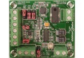
5 terminal blocks are used for all external connections for easy set-up and use a fairly large part of the PCB surface. The PCB measures only 56.5 x 50.2 mm. Tantalum decoupling capacitors C9 and C10 together can handle the 2 A maximum switching current from the driver. LED1 indicates input voltage is present. There’s a tolerance in the frequency that can be set with trimmer P1. We measured 16 to 48 kHz. Put the trimmer in mid-position, setting the frequency in any case to more than 20 kHz. This is the minimum frequency specified for the BD6222 (maximum is 100 kHz). Resistors R9 and R10 make sure no input of the multiplexer is left open if no signal is applied to K1. Minimum current consumption of the circuit 11.2 mA (no connections to K1 and pin 3 of K2, pin 2 of K2 tied low and PD set to low). If R1 isn’t connected to any control voltage (pin 2 of K2 open and IC3 in power-down mode) than the input voltage of IC1 is either 1.68 V (5 V range, jumper JP2 closed) or 1 V (10 V range, jumper JP2 open). Both are within the control range of the SG3524D and current consumption in both cases will be higher (14 -15 mA).
Testing the A/D converter can be done by using our FT311D Break-out Board ( project 130516). The I2Cdemo utility of FTDI is basic but very useful to quickly test the A/D converter. The device address is set to 0001100 by setting A0 and A1 to 0 (JP5 and JP6 respectively). To set the output voltage only three fields need data to be entered: Device Address, Address (MSB byte) and Write Bytes. If for instance 0C, 0F and F0 are entered respectively and send the output of the DAC will be set to its maximum output voltage. IO0 is SCL and IO1 is SDA. From jumper JP1 on the FT311D Break-out Board only CFG2 need to be closed to set the FT311D in I2C mode.
Measurements from our first two prototypes and specifications (+5V = 4.93 V)
Power supply 12 V
Maximum output current 2 A
Minimum supply current 11.2 mA
PWM control range 0 – 100 %
External control voltage 0.16 V (PWM 0 %, 5 V range)
4.88 V (PWM 100 %, 5 V range)
0.27 V (PWM 0 %, 10 V range)
9.7 V (PWM 100 %, 10 V range)
Input impedance (pin 2 of K2) 6.43 kΩ (5 V range)
15.36 kΩ (10 V range)
Bill of materials
Resistor
R1 = 2.7 kΩ, 5%, 0.1W, 150V, SMD 0805
R2 = 8.2 kΩ, 5%, 0.1W, 150V, SMD 0805
R3,R4 = 11 kΩ, 5 %, 0W1, 150 V, SMD 0805
R5 = 5.6 kΩ, 5%, 0.1W, 150V, SMD 0805
R6 = 2.0 kΩ 1 %, 0W125, 150 V, SMD 0805
R7 = 330 Ω, 5%, 0.1W, 150V, SMD 0805
R8 = 4.7 kΩ, 5%, 0.1W, 150V, SMD 0805
R9-R14 = 10 kΩ, 5%, 0.1W, 150V, SMD 0805
R15 = 2.2 kΩ, 5%, 0.1W, 150V, SMD 0805
P1 = 5 kΩ, trimmer, 4.5 mm, 250 mW, SMD
Capacitor
C1 = 10 nF, 50 V, X7R, SMD 0805
C2,C4,C6,C7,C8 = 100 nF, 50 V, X7R, SMD 0805
C3 = 10 µF, 16 V, X5R, SMD 0805
C5 = 47 µF, 6.3 V, 0.5 Ω, tantalum, SMD case B
C9,C10 = 220 µF, 16 V, 0.1 Ω, tantalum. SMS case E
Semiconductor
D1,D2 = TS4148 RY, SMD 0805
LED1 = LED, green, 50 mcd, 2.1 V @ 20 mA, SMD 0805
IC1 = SG3524D, SMD SOIC-16
IC2 = MC74HC4053ADTG, SMD TSSOP-16
IC3 = AD5301BRMZ, SMD MSOP-8
IC4 = BD6222FP-E2, SMD HSOP-25
Other
K1A,K1B,K2 = 3-way terminal block 5.08 mm
K3,K4 = 2-way terminal block, 5.08 mm
JP1,JP5,P6,JP7 = 3-way pinheader, vertical, pitch 2.54 mm
JP3,JP4 = 2-way pinheader, vertical, pitch 2.54 mm
JP1, JP3-JP7 = Shunt jumper, 2.54 mm spacing
Misc.
PCB 140562-1 v1.1
Discussion (0 commentaire(s))