
Digital key
Digital lock with USB key insertion and code via keypad
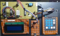
The project refers to a digital combination lock through the insertion of a suitably modified USB stick. Referring to figure 1, the project is based on two MCUs of the 18F252 type which for simplicity we will call U2 and U3.The U2 manages the 4x4 matrix KeyPad where in addition to the numeric buttons there are other buttons whose function will be explained later when we go into detail about the individual functions.U2 interacts with U3 through the four ports called port C0-1-2-3 (pin 11-12-13-14), connected to the respective ports of U3 called port C7-6-5-3 of pins 18-17-16 -13 to be able to transmit information about the pressed button. The two ports C5 C6 (pins 16 and 17) of U2 are connected to the two ports A1 A0 (pins 3 and 2) of U3 necessary for the dialogue between them, based on an RX/TX type protocol justified as in figure 2.The U3 has the heaviest job, in fact in addition to acquiring the information of the pressed button it manages everything relating to the management of the Service Mode and the Operational Mode and the management of the LCD screens of the LM044L 4x20 type and the useful relay to have a voltage at the right moment or to drive an electromechanical device. All of this explained further on. The USB stick has a card inside with an EEPROM memory of the 24LC32A type (figure 3) divided into pages. The system uses the first 128 cells of page 0, therefore from cell 0 to cell 127. For regarding the connection of the pen to the system, the functionality of the 4 pins of the key must be specified.Pin 1 is used to power the memory. Pin 2 and pin 3 are used for connection to the U3 ports respectively at pin 14 (SCK) and pin 15 (SDA) for using the i2c protocol. While pin 4 which is connected directly to pin 1 is used to alert the system that the key has been inserted into the CN3 connector.Pin 11 of U3 called port C0 is programmed into input, and forced to a low level (logical 0). When the key is inserted on pin 11, 5 volts from pin 4 of the key arrive, forcing the port to a high level (logical 1). This change in logical state from 0 to 1 is interpreted by the system as the presence of the key. INSERTING THE PIN INTO THE KEY AND ITS ENCRYPTION
It's the first thing to do. The 24LC32a EEPROM has r/w memory divided into pages. The system uses the first 128 memory cells of the first page (page 0) therefore from cell 0 to cell 127. Of all the cells used, only 5 of them contain the value of the single digit that makes up the PIN, the others will contain a random value from 0 to 9 recorded via algorithm based on the PIN itself. The cells of the pin are positioned discontinuously hidden among the 128 cells and not in sequential order, for example if the pin is 12345 if you are aware of the dedicated cells and they are read in sequence you could for example have 24153 as an answer. Only the system is aware of the reading key by identifying the 5 cells and the order in which to read them. In figure 4 you can check the contents of the 128 cells of the eeprom after entering two different PINs.The images were extrapolated from the Proteus 8.9 program used for the theoretical design.In figure 5, however, we can see the image on the left, again extrapolated from Proteus, regarding the mapping of the eeprom after entering the PIN 49088 and the related code generated. On the right, images of the LCD display in the practical phase regarding the PIN and mapping.As regards the CODE, the latter is generated temporarily only at the necessary moment, during insertion on request or during display, after which it is deleted from the system variables. SERVICE MODE
This menu can be recalled by setting the SW1 dip switch connected to port A2 (pin 4) of U3 to open. From the electrical diagram it can be verified that when the SW1 is open and therefore the service mode is called up, the circuit composed of the resistor R19 and the LED D1 are powered correctly as there is a 5 Volt voltage upstream of the resistor and downstream of the LED 0 Volt, a situation that allows LED D1 to light up. While the circuit composed of the LED D2 and the resistor R20 is located both upstream and downstream with a voltage of 0 Volts, a situation which does not allow the LED to light up. By closing SW1, thus recalling the operating mode state, explained further on, we will find ourselves with the R19 - D1 circuit with a voltage of 5 Volts both upstream and downstream, and in these conditions the LED cannot light up. Instead, the D2 - R20 circuit is found upstream with a voltage of 5 Volts and downstream with 0 Volts, a situation which allows LED D2 to light up.When for service reasons it is necessary to switch from an operational state to the service state or vice versa, in addition to using the SW1, a reset is necessary by acting on the P1 button which leads through the divider formed by R16 - R17, in the pull-up and pull configuration respectively -down, the MCLR gate (pin 1) of U3 goes from a logical 1 state to a logical 0 state to return to a logical 1 state when P1 is released.The service mode menu includes three items that can be recalled by pressing one of the keys 1 – 2 – 3. (figure 6)
Button 1: R/W KEY
By selecting this item you can view the stored PIN on the display and the code that is temporarily generated with the characteristics described above to be entered at the time of the request. Or you can enter a new PIN. After selecting this item, the screen in figure 7 will be displayed.On the left we find a field made up of 5 pixels enclosed by square brackets. The writing immediately below clarifies that the new PIN must be entered in that field.On the right in the column we have the PIN currently present in the key and the CODE generated after reading the PIN. With the items present in the fourth line we can return to the menu as in figure 7 by pressing the CL key or enter a new pin by pressing the OK key. With the CL key wherever we are in both service mode and operational mode we return to the previous phase. The system does not accept the entry of the five digits with the same numerical value (17854 correct, 44444 incorrect).Once you have pressed the OK button you can enter the new PIN in the field above the wording "new PIN". Once entered and confirmed by pressing the OK button.In this phase the system inserts a value from 0 to 9 into the memory cells depending on the PIN entered and the digits of the new PIN into the five cells. The five digits that compose it are entered according to the order procedure as previously described. Once this phase is finished, the system will read the PIN digits again to give an overview of the quality of the work performed and that everything went ok.
Button 2: CLEAR KEY
With this entry you delete all 128 cells by inserting a hexadecimal value FF. Immediately after the deletion is finished, the first part of the key mapping will be displayed as in figure 9. You can check the second page of the mapping by pressing the up arrow key or the CL key to return to the menu.
Button 3: VIEW MEM
By selecting this item, the system will read the 128 cells displaying the numerical value contained therein arranged in two screens, page 1 composed on the left by lines from 0 to 3 which contain 8 cells each, on the right by lines from 4 to 7 which contain 8 cells eachpage 2 composed on the left by rows from 8 to 11 which contain 8 cells each, on the right by rows from 12 to 15 which contain 8 cells each .By default, the first page displayed is page 1, which includes cells from 0 to 63, while page two includes cells from 64 to 128. To move from one page to another, use the two buttons with the arrow symbol (see figure 8). To return to the menu, press the CL key.Before moving on to operational mode, some considerations must be made on some parts present in the diagram electric. The CN3 connector which "accommodates" the key is interfaced with the U3 pins by a series of schottky diodes.Even if the ports of the integrated circuits normally have their own internal protection, it is convenient to insert diodes on the outside to avoid "stressing" the internal protections too much, avoiding damage due to extra voltages.The ASM1117 module powers the LCD LEDs with a stabilized voltage of 3.3 Volts.As regards Q1, a 2N3904 type npn transistor configured as an inverter gate is used to reset U3. When turning on the two MCUs do not synchronize, displaying random characters on the display without any interpretation. A few seconds after switching on, port C7 of U2 (pin 18) configured in out and forced low, and connected via resistor R12 to the base of the transistor, is set to a high level and then returns to a low level. A high level is present via the poll-up resistor R13 on the collector. When this high-low-high variation occurs, the collector connected to pin 1 of U3, via the emitter, finds itself "short-circuited" to ground and then finds itself again at a high level and Q1 again blocked, effectively replicating what happens by temporarily pressing the P1 button.The unused pins of both U2 and U3 are all connected to ground and programmed to input. To prevent the doorsunused they pick up any electrical disturbances, being structured with MOS technology they are very sensitive to external disturbances, adopting the virtual GND method, i.e. connecting them to ground to avoid these phenomena.in the event of doubts about the reliability of the power supply then it is advisable to insert pull-down resistors. OPERATIONAL MODE
È lo Stato a dimostrare l'utilità di questo progetto. Inserendo la chiave nel connettore CN3, il sistema, come già spiegato, rileva la presenza della chiave e legge le 5 celle che contengono le cifre del PIN, generando il codice. Ora bisogna inserire le cinque cifre che compongono le CODE. Anche in questa fase è possibile tornare indietro premendo il pulsante CL. Il CODICE è corretto se il programma confronta il CODICE temporaneamente memorizzato nella variabile con quello inserito e sono identici. In questo caso la porta A5 (pin7) di U2 programmata in out e mantenuta a livello basso (0 logico), commuta il suo stato da livello basso a livello alto (1 logico) portando in conduzione un transistor tramite R27 collegato alla base di Q2 npn del tipo 2N3904 e eccitando il relè RL1. Dopo circa 2,5 secondi, la porta A5 ritorna a un livello basso, provocando nuovamente la disattivazione di Q2 e la diseccitazione di RL1. Ovviamente, se il CODICE inserito non corrisponde a quello presente nella variabile, il display indicherà che il CODICE inserito non è corretto e il sistema vi chiederà di scollegare la chiave. Per quanto riguarda il software utilizzato per gestire i due PIC, il più semplice Mikrobasic Come progettazione è stato utilizzato il software di assemblaggio 7 secondo il mio modo di operare. Basti pensare che il listato per U3 è composto da circa 2300 righe di istruzioni in Mikrobasic mentre in assembly sono circa 6500. Per programmare i PIC è stato utilizzato PICKIT3.
Discussion (3 commentaire(s))