
USB-RS232 converter (FT231X BoB) [180537]
Next generation USB/Serial Bridge/BOB using a FT231XQ, normal pin headers and a Micro-USB connector. VCCIO is +1.8..3.3 V but 5 V UART logic tolerant.
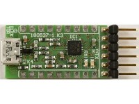
In 2011 we published a small PCB, FT232R USB/Serial Bridge/BOB (110553) with a USB-UART IC from FTDI, the FT232RQ. Here we present its successor with a cheaper version, a FT231XQ. But there are some other changes too. Normal pin headers can be used now. The (optional) two connectors on the long sides of the PCB are placed a little closer together, row distance 12.7 mm instead of 15.24 mm. The new PCB is just a fraction longer, 29.2 mm instead of 27 mm. With a right-angled pin header mounted on K2 total length from Micro-USB connector to the end of K2 is approximately 39 mm. The width with connectors mounted to the sides of the old BoB is wider than the new version since now the connectors are mounted completely underneath the PCB. So, width of the new BoB is always the width of the PCB, 15.24 mm. We changed the order of the signals of the connector at the end of the PCB (K2) and added signal RTS to be compatible with the USB-RS232 cables from FTDI. Additionally, all UART signals are now available on one side (K3). Power supply connections, Reset and configurable CBUS I/O’s (the FT231 has one I/O less) are available on the other side (K4). The Mini-USB connector is replaced by a Micro-USB version since this type is more common these days. Also, an ESD protection circuit (D1) is added to the data lines USB connector. Just to be save. For properties of the FT231 we refer to the datasheet (at time of writing this version 1.2, https://www.ftdichip.com/Support/Documents/DataSheets/ICs/DS_FT231X.pdf). But also have a look at technical note TN_140 (https://www.ftdichip.com/Support/Documents/TechnicalNotes/TN_140_FT231X%20Errata%20Technical%20Note.pdf).
The new BoB also has two LEDs to indicate data transfer. The LED’s are connected to CBUS1 and CBUS2. By default, these I/O’s are configured for RXLED# and TXLED# respectively and indicate USB data is received (LED2/RX) or transmitted (LED1/TX). If you prefer the LEDs indicating RS232 data transfer this can easily be configured with a special utility called FTPROG (https://www.ftdichip.com/Support/Utilities.htm#FT_PROG), the functions can be swapped. Or maybe you don’t care, in either case there’s a LED blinking. With FTPROG several settings can be changed. But be careful this can also make the chip become unresponsive.
The PCB is a two-layer PCB with 0603 resistors and capacitors and more than a few vias. Because of this there’s barely room for references and the reason they are placed inside the footprint of the resistors and capacitors (and D1). If a bare PCB is to be mounted and soldered by hand just use an enlarged top overlay, so you’ll know where these components are located. A tip you may want to leave mounting D1 till the end, until Micro-USB connector K1 is mounted. Short circuits between the pins of K1 are hard to remove once D1 is mounted. After mounting all components check all connector pins for short circuits, especially between the USB connector pins. To avoid the label TX on PCB becoming unreadable it’s moved to the side of the LED. So, this label TX is not a name for the pin of K2 next to it (that’s VCCIO).
There are two 0-ohm resistors of which the footprint is designed to act as a solder jumper as well. If the resistor is removed (R1 and/or R8) a resistor is not needed again. The two pads of this footprint are placed very close together and can easily be connected just using solder. R1 can be removed if the BoB is to be used in self-powered mode. Virtually no current is drawn then from the +5V of K1. Only 0.2 mA by resistor divider R4/R5 to detect the unplugging of the USB connector. This mode can be set with FTPROG. An external power supply must be connected to pin 1 of K4. Be careful, this pin is directly connected to the VCC of IC1. R8 connects the power supply VCCIO (pin 4 of K4 and pin 3 of K2) for the IO cells to the internal +3.3 V voltage regulator, available at pin 3 of K4. VCCIO is specified for a supply voltage of +1.8 to +3.3 V, with an absolute maximum of +4 V. Never connect +5 V to VCCIO! This will destroy the FT231! This is an important difference with the previous Bob (110553). It is stated that the input is 5 V tolerant however, e.g. external UART logic working on a higher power supply voltage can be connected safely.
An image of the BoB with all pin names can be found under downloads. All pads of K2, K3 and K4 extend to the edge of the PCB. This way, designing a dedicated footprint, the BoB can be soldered directly on top of another PCB manually, in case you don't want to use pin headers. The exposed pad of IC1 is connected to ground an has no solder mask on the bottom layer.
A few things about RS232
The most basic RS232 connection between two devices is null modem, also called crossover. TxD is connected to RxD and vice versa and of course ground of both devices are connected. Beside 5, 6, 7 or 8 data bits, a start bit, maximal two stop bits and a parity bit are used.
A more secure way of transmitting data is the use of a buffer to store data temporarily. Handshaking either by hardware or software prevent a buffer overflow. Hardware handshaking uses additional signals DTR, DSR, RTS and CTS for control. CTS is cross connected to RTS and DTR is cross connected to DSR. In case of a modem also DCD and RI are used, DCD to DCD and RI to RI.
Software handshaking uses two ASCII characters for start-stop communication and called software flow control. It uses two control characters: XON and XOFF, decimal 17 and 19. This has a draw back. In case of binary data these characters cannot be used, or software handshaking is not possible then.
Testing the BoB can be done by use of terminal program like HTerm. Of course, easiest way is using two computers and two BoB’s. When using full handshake, the connection can be checked in HTerm. Green indictors light up when DTR and/or RTS on the other side are enabled.
Most important properties:
Micro-USB connector
USB 2.0 Full Speed capable
VCCIO +1.8...+3.3 V (4 V abs. max., 5 V input from UART logic tolerant)
+3.3 V regulator output, 50 mA max.
Data transfer 300 baud to 3 Mbaud
USB to full handshake UART
Compatible with RS232, RS485 and RS422
I/O pin output drive 4 mA min., 16 mA max.
4 configurable CBUS pins
More information can be found in the original article FT232R USB/Serial Bridge/BOB (110553):
https://www.elektormagazine.com/magazine/elektor-201109/19727
More about RS232:
https://www.commfront.com/pages/3-easy-steps-to-understand-and-control-your-rs232-devices
https://www.codrey.com/embedded-systems/rs232-serial-communication/
Drivers:
https://www.ftdichip.com/Drivers/VCP.htm
https://www.ftdichip.com/Drivers/D2XX.htm
Bill of Materials
Resistor
R1,R8 = 0 Ω, 75 V, 100 mW, SMD 0603
R2,R3 = 27 Ω, 75 V, 100 mW, 1 %, SMD 0603
R4 = 10 kΩ, 50 V, 100 mW, 1 %, SMD 0603
R5 = 15 kΩ, 50 V, 100 mW, 5 %, SMD 0603
R6,R7 = 270 Ω, 50 V, 100 mW, 1 %, SMD 0603
Capacitor
C1,C5 = 10 nF, 50 V, 20 %, X7R, SMD 0603
C2,C3 = 47 pF, 50 V, 2 %, C0G/NP0, SMD 0603
C4,C7,C8 = 100 nF, 50 V, 10 %, X7R, SMD 0603
C6 = 4.7 µF, 6.3 V, 10 %, X5R, SMD 0603
Inductor
L1,L2 = 330 Ω @ 100 MHz, 1.7 A, 0.08 Ω, Murata BLM18KG331SN1D
Semiconductor
D1 = PRTR5V0U2X, ESD Protection Device, SMD SOT-143B
LED1 (TX) = HSMG-C190, led green, SMD 0603
LED2 (RX) = HSMS-C190, led red, SMD 0603
IC1 = FT231XQ, SMD QFN-20
Other
K1 = Micro USB type B, receptacle, SMD
K2 = 6-way pin header SIL, 2.54 mm pitch, right angle
K3,K4 = 9-way pin header SIL, 2.54 mm pitch, straight
Misc.
PCB 180537-1 v1.0
Discussion (0 commentaire(s))