
High-Precision Capacitance Meter
The proposed measurement principle is based on constant current, making the measurement completely insensitive to the series resistance. The output of the capacitance-to-time converter can either be measured and directly displayed with a universal counter, or with a simple microcontroller-based counter proposed here. The achievable accuracy is primarily limited by the precision resistors used.
Introduction
The proposed high-precision capacitance meter ("C meter") is based on charging the unknown capacitor (or "DUT") with constant current, leading to a voltage rise linear in time. The time interval between passing two symmetric reference voltages is directly proportional to the capacitance. When using the same reference voltage in combination with precision resistors to generate the charging current, the absolute value of the reference voltage cancels out in the resulting time interval.
Due to the constant current used, the measurement is completely insensitive to the series resistance of the DUT. In contrast to LCR meters, no "short" calibration is required; depending on the measurement setup and the capacitance value, an "open" measurement may be necessary to cancel parasitic capacitances.
Using appropriate values for the resistors, the output signal of the C meter can be measured and the result displayed directly (i.e. without calibration factor) using a universal counter. Alternatively, a simple microcontroller-based counter is proposed to measure the time interval and display the result.
Depending on the details of the employed electrical circuit as well as the measurement range and the capacitance value, the achievable accuracy is primarily limited by the precision resistors used. An accuracy better than 0.1% is readily achieved using a reasonably complex design and at affordable costs. Using a carefully optimized design including auto-calibration of all relevant offset voltages etc. and the best available (and thus costly) components, the ultimate potential for the achievable accuracy is in the order of 0.01%.
The attached basic schematic illustrates the measurement principle of the proposed
C meter:
The unknown capacitor Cx and the precision FET-input operational amplifier form an integrator integrating the input current I = Uref/Rm; the polarity of the reference voltage Uref is changed periodically using an analog switch. The auxilliary comparators 1 and 2 compare the output of the integrator with about twice Uref and switch the RS-flipflop 1, which controls the polarity switch. The resulting output Uint of the integrator is a triangular wave with a peak-to-peak amplitude of approx. 4Uref and a period of approx. 8RmCx.
The precision comparators 3 and 4 compare the integrator output Uint with +Uref and -Uref, respectively, and switch RS-flipflop 2, which generates the output signal for the measurement of the time interval. Depending on the polarity of the comparators, either the rising or the falling part of the integrator signal is evaluated.
Improvements of the basic setup
The second attached schematic shows the first improvement of the basic measurement principle:
A second analog switch is added, enabling to switch the reference voltage for comparator 5, depending on the polarity of the integrator output, which is detected by comparator 6. The single comparator 5 replaces the comparators 3 and 4, thus eliminating any inaccuracy due to unequal offset voltages of the two comparators, being one of the major potential error sources of the basic principle.
Since the output signal of comparator 5 is slightly more complex, a D-flipflop is employed instead of RS-flipflop 2. The AND gate is used to select the rising part of the integrator signal only. If needed, a second D-flipflop and AND gate can be added to offer a second output for the falling part of the signal.
The third attached schematic shows a second improvement:
The differential comparator 5 is replaced by a precision difference amplifier followed by the ground-referenced comparator 7. In fact, a summing amplifier is used instead of a "true" difference amplifier; this can be accomplished by inverting the signal from the second analog switch AS2 by inverting its digital control signal (not shown). Due to this, the inputs of the fast operational amplifier are at exactly the same (virtual) ground level during both "zero" transitions at +/- Uref to be detected; this eliminates any common-mode dependent variations of the offset voltage.
In fact, the precision requirements for the OP and comparator 7 are quite low; therefore, high-speed models can be used. On the other hand, the precision of the four input resistors R1 is critical and can be guaranteed best by using a precision R-network with very tight matching of the resistor values (e.g. 0.01% max) as well as tight TCR matching (e.g. 1ppm/K max). The second fast OP, which amplifies the signal from the second analog switch AS2 by -1/2, is used in combination with two Schottky diodes to clamp the integrator signal Uint at a level as close as reasonably prossible to the zero transitions. This allows to operate the summing amplifier at a substantial gain |G| = R2/2R1 (e.g. 7-10) without saturating its output. Provided that the slew rate of the OP is sufficiently high, this further reduces the requirements for comparator 7.
The fourth attached schematic shows a third improvement:
Since the input current I of the integrator is proportional to the voltage difference DeltaU = Uref - Uoffset, its accuracy depends on the input offset voltage Uoffset of the FET-OP. The static offset voltage can be minimized either by choosing an appropriate precision OP (e.g. OPA192) having a sufficiently low offset (e.g. 5µV typ), or - if necessary - by measuring the actual offset and applying the inverse voltage (-Uoffset) to the non-inverting input of the OP.
Unfortunately, a dynamic offset also exists, which is roughly proportional to the actual slew rate dU/dt of the output signal and inversely proportional to the gain-bandwidth product GBWP of the OP. This effect is most significant at small capacities Cx and high charging currents I. Straightforward solutions would be either to limit dU/dt (e.g. by defining a lower limit for Cx depending on Rm), or to use an OP with sufficiently high GBWP.
The first option would reduce the useful measurement range(s) of the C meter whereas the second would reduce the overall accuracy of the device since fast OPs typically have worse DC specifications (e.g. offset voltage drift, open loop gain etc.) than precision OPs. Additionally, using a fast OP would lead to a lower threshold for parasitic oscillations due to the series inductance of Cx and the wiring of the test fixture.
The proposed solution is to add a fast booster OP at the output of the precision FET-OP (but inside its feedback loop). The DC specifications of the booster OP are uncritical; it should have a high slew rate and a fast (much faster than the precision OP) settling time. The low-frequency gain of the booster amplifier, which is controlled by the ratio of the resistors R4 and R3, is typically in the order of 100-500 and reduces the dU/dt and thus the dynamic offset of the precision OP by the same order of magnitude. The high-frequency gain, which is controlled by C1 and R3, has to drop fast enough with increasing frequencies to maintain a phase margin of at least about 40deg.
Detailed description of the modules
The last attached schematic shows an overview of all on-board modules of the C meter, including a module with all comparators, the logic block, and the on-board power supply as well as the connectors.
J101 is a 16-pin connector for a (shielded) ribbon cable connecting the C meter, which should be placed in a separate metal housing (e.g. Hammond 1590B2), with the optional counter module described in a separate contribution (see below), which remotely controls the range selection and makes available all relevant digital measurement signals (e.g. from the rising and from the falling slope of the integrator signal separately, as well as a combined signal from both slopes, either transmitted as isolated 5V signal or as LVDS signal. 5 jumpers (JP9, JP10, and JP11) select between internal and external control of the measurement ranges; the counter module is used for the external control.
The fifth attached schematic shows a symmetric voltage reference for the C meter:
As mentioned above, the absolute value of the voltage reference (here: 2.5V nominal) is uncritical, but its symmetry (i.e. equality of positive and negative voltage) should be excellent, showing low drift with temperature and time. Furthermore, its dynamic impedance should be as low as possible to minimize the voltage peaks occuring when the analog switches,,having some parasitic capacitances,as well as some charge injection, are turned on and off.
Although it is possible to use a "conventional" voltage reference (e.g. REF5025), having a relatively high dynamic impedance, and to buffer it either with large capacitors or - more - practicable - using a buffer amplifier realized with one or more adequate separate OPs (such a design is available on request), it is much simpler (and cheaper) to use a voltage reference with integrated buffer amplifier having a low dynamic impedance like REF6025. Using adequate output capacitors, (low ESR MLCC with high resonance frequency), its output impedance is below 25mOhm from DC to at least 1MHz (see Fig. 16 of the datasheet).
R1 is required to keep the output current of REF6025 within its nominal range of +/-4mA; its actual value depends on the load. OP LTC6228 is configured to invert the reference voltage; due to its excellent dynamic properties, it shows a low dynamic impedance comparable to that of REF6025 at its output. The drawback of this OP is its very high input bias current (-16µA nom.; which can be reduced to +/- 2.5µA when using the integrated bias cancellation) and the resulting high input offset current (+/-0.55µA at 25°C, which is even incrasing to 0.9µA when enabling the bias cancellation!).
Therefore, the input impedance of the inverting and the non-inverting input should be kept as low as possible and have to be balanced well to minimize temperature drift; thus R6 is used to balance R5||R2. R2 and R5 should be matched as good as reasonably possible (e.g. by using a precision R-network like LT5400-4), but there still may be some need for accurately adjusting the negative reference voltage relative to the positive one. In principle, this can be done using a trimmer (e.g. 1MOhm parallel to R3 or R5), but a more compact (and cost effective) solution may be to add some small series resistors (R4, R3 and R7) to R5, R2, and R6.
The shown (solder) jumpers JP1-3 are useful to test the output voltage without series resistors (and to measure the actual values of the resistors R5, R2, and R6 when soldered in place) and to choose and solder in the appropriate resistors accordingly. Please keep in mind that R7 has to compensate the 1Ohm lower than needed nominal value of R6. 1-2Ohm is a good target range for R4 and R3, R7 will be in the 1.5-2Ohm range in this case.
The sixth attached schematic shows the analog switches including buffer amplifiers and range switches:
The analog switches should have low capacitances, low charge injection, and short switching times; the chosen ADG719 is not only very fast, but offers a low on-resistance (not necessary in this case) at the same time. Please note that this switch has a voltage range of 5V (or +/-2.5V) only, which is sufficient for the chosen reference voltage (similar switches for higher voltages are somewhat slower, but can be employed also, if necessary). The resistors R1, R4, R14, and R17 are limiting the charging current of the parasitic capacitances of the switches, which minimizes the effect of switching on the reference sources.
Additionally, the slew rate of the voltage steps is limited by C1 (C4) in combination with R3 (R15) and R1/R4 (R14/R17) to prevent massive overdriving of the subsequent amplifiers. Due to the relatively low impedances of the loads, the switched signals are buffered by precision OPs; the chosen OPA827 is the best compromise in terms of speed and accuracy; OPA192 would be more accurate, but slower, and OPA828 is faster, but less accurate (fast bipolar OPs could be employed, but need more care to minimize the inaccuracies due to their input currents).
In the proposed circuit, the reference voltage for the input of the integrator is doubled to +/-5V by the buffer amplifier. Due to this, the input resistor Rm (R2 etc.) has to be doubled too, to achieve the same input current I. The advantage is a lower influence of the (dynamic) input offset voltage of the integrator on the current I. Of course, the gain of the buffer amplifier has to be very accurate to avoid a loss of overall accuracy. Therefore, a precision R-network (LT5400-4) is used as voltage divider; depending on the targeted accuracy, either the B- (0.025%) or the A-grade (0.01% matching) of the network has to be used. If necessary, trimming can be performed additionally, e.g. using small series resistors (as in the voltage reference).
The schematic shows 3 different measurement ranges with Rm of 10kOhm, 100kOhm, and 1MOhm. In constrast to 10kOhm resistors with 0.01% tolerance and low TCR, as employed for R2, which are readily available at reasonable costs, the higher values are typically difficult and/or very expensive to buy with the required specs. Therefore, the proposed alternative is to use pairs of cheaper 0.1% resistors with 49.9kOhm and 499kOhm (and low TCR!) instead, and to add small series resistors (R8: 0-400Ohm; R12: 0-4kOhm) to achieve the required values with high accuracy. To do so, the actual values of the resistor pairs (already soldered in place) have to be measured with sufficient accuracy and the series resistors have to be chosen and soldered in accordingly.
The ranges are switched using PhotoMOS relays, (AQY221), having a product of off-capacitance and on-resistance lower than any conventional analog switch (but higher than reed relays). The trade-off is a low switching speed, which is no disadvantage is this application. Like a mechanical relay, a PhotoMOS relay has a true isolation barrier (optically coupled) with low coupling capacitance between the control input and the switch. Due to this, the measurement ranges can be controlled by the counter module without galvanic connections, thus minimizing electromagnetic interference. The isolation remains intact when using the isolated 5V signal for transmission to the counter.
The PhotoMOS relays are available with lower on-resistance, but higher off-capacitance (suffix R2V), as used to switch R2, and vice versa (suffix N3V), used for switching the higher resistance values.
The seventh attached schematic shows the complete integrator including all protective elements:
The input of the integrator is protected by the low leakage current diode pair D6 (BAV199) and the current limiting resistor R17. C17 is used to minimize the detrimental effects of R17 on the high-frequency performance of U6. The output of the integrator is protected by the diodes D1 and D2 and the current limiting resistor R18. Please note that the protection is limited to approx. 30V when the C meter is on (10V when off) and for discharging capacitors having a few µF maximum (not tested yet, no guarantees!); therefore it is strongly recommended always to discharge Cx before connecting it to the C meter.
A buffer amplifier (U7) is employed to decouple the integrator from the fast comparator used for the "zero" transision detection, which feeds back high-frequency distortions when passing the transition. Please note that a (voltage independent) offset voltage of this amplifier does not affect the measurement accuracy, since a time interval for reaching a certain voltage difference (and not a single voltage) is measured.
The C meter can operate at repetition rates as high as 250 kHz, but its accuracy (as well as the relative resolution of the time interval measurement) is best at repetition rates of approx. 25kHz, corresponding to 1nF in range 1 and to 100pF (10pF) in range 2 (3), or lower. When measuring capacitances below these values, it is recommended to use "minimum" (or offset) capacitors in parallel to the DUT; for this purpose two such capacitors (C9 having 1nF and C7 having 100pF) are located on the PCB, which can be selected using jumper JP2. In this case (or when Cx is small, or when a test fixture with significant parasitic capacitance is used), an "open" (or offset) measurement has to be performed prior to the measurement with Cx in place. The difference of the results of both measurements is the capacitance of Cx; the counter module described separately can perform the suptraction automatically.
Measurement durations longer than approx. 100ms may also lead to less-than-optimal accuracy, depending e.g. on the time constant of the DUT (Cx times its parallel resistance Rp); this correponds to a maximum capacitance of approx. 10µF in range 1 (1µF and 100nF in range 2 and 3, respectively). Parallel resistances Rp of less than 5MOhm in range 1 (50MOhm and 500MOhm in range 2 and 3, respectively) will lead to significant measurement errors (>= 0.05%). (As mentioned already, due to the constant current used, series resistances of the DUT of up to at least 200Ohm in range 1 (2kOhm and 20kOhm in range 2 and 3, respectively) will not affect the measurement result at all.)
A further attached schematic shows the details of all comparators used in the C-Meter:
The auxilliary comparators, which do not need to be very accurate but quite fast, are realized using the dual comparator LM319. D301 and D302 are employed to split the input voltage range, which is necessary to limit the voltage difference at the inputs of the comparators.
The main comparator is consisting of the precision difference (or summing) amplifier already described above, an intermediate amplifier realized using OPA695, and two alternative fast comparators U303 and U307. The first (LTC6752-3) generates in combination with the Schmitt trigger inverters U302 and U305 complementary 5V signals, whereas the second (LMH7220) has complementary LVDS outputs. Both amplifier stages are equipped with Schottky diode pairs for clipping their output signal; this avoids saturation or overdriving of the subsequent stage.
The last two comparators U308, realized using the dual comparator TLV3502, are needed to switch the reference voltage (AS2) of the main comparator (one for each slope). Both have a reference voltage of +/-1.25V, which allows to switch the main reference voltage already before the integrator signal (Int_out) crosses zero. This allows to settle the main reference signal as early as possible and thus before the integrator signal crosses the main reference voltage.
Another attached schematic shows the logic block of the C meter:
The logic block consists of the flipflops (FF), the output circuits, and the internal range selection.
The first FF U1A (74AHC74), which is configured as RS-FF, controls the polarity of the reference voltage for the integrator by sending its output signal (Up) to the control input of analog switch AS1.
The pair of D-FFs U19 (the second 74AHC74) in combination with the AND gates U18A and B is used to extract the complementary time interval signals for the rising and the falling slope of Int_out from the output signal of the main comparator. The subsequent OR gate U20 combines both signals. Please note that for the LVDS signals this proccessing is performed in the separate counter module.
The last FF U1B, which is configured as RS-FF also, is used to control the switching of the reference voltage (AS2). The discrete components added to this FF avoid the case that both inputs are LOW at the same time, causing an undefined (or "racing") condition.
The isolated 5V signals are supplied using U9 (ADuM120N1 or ADuM1200(W)UR). Two different signals can be supplied at the same time: Either the signals from the rising and the falling slope (U and D), or the combined signal and its complement (C and /C). JP7, which can be easily replaced by an external switch if needed, in combination with the 2:1 demultiplexers U16 and U22 performs the selection of the signals. Again, the processing of the LVDS signals is performed in the external counter module; therefore, the corresponding output signals are available at this module only. To enable the LVDS signal processing, the slope signal (Up) has to be available at the counter module; consequently, it is transmitted as a LVDS signal also. The required signal conversion is performed using the LVDS transmitter U30 (DS90C401) in combination with the fast analog switch U29 (DG419) used as level shifter.
The internal range selection is performed using U23 (74HC4017), a decoded 5-bit Johnson counter; the counting limit is set to "2" by connecting Q3 with the reset input. For changing the range, a pushbutton connected to the clock input (Range_sw) has to be pressed; optionally, the actual range can be indicated by 3 LEDs connected to Q0-2.
Finally, another schematic shows the on-board power supply, including the necessary blocking capacitors.
The C meter requires the following power supplies: +/- 10V for the precision OPs, +/- 5V for the fast analog components, and +/-2.5V for the logic circuits. The +/- 5V supply is generated by the internal low-dropout voltage regulators U501 (LT1964-5) and U502 (LT3062-5). To minimize the on-board heat generation, which detrimentally affects the achievable accuracy, they need a +/-6V nominal supply, which easily can be derived from the +/- 10 V supply using a few diodes (e.g. 1N4007) in series inside the external power supply.
Together with the dynamic impedance of the power supplies and the layout of the PCB, the choice and location of the blocking capacitors is critical for the optimal performance of the C meter. The +/-5V supply is placed on the PCB since a low dynamic impedance (e.g. approx. 200mOhm in the case of LT1964-5 with 10nF bypass capacitor) of the voltage regulator, which is desirable for accurate operation of the critical fast components, requires very short traces (e.g. < 2 cm) to avoid strong resonances within the critical frequency range (up to about 100 MHz) due to the parasitic inductances of the traces in combination with the blocking capacitors, leading to severe ringing on the power supplies when supply currents are changing rapidly.
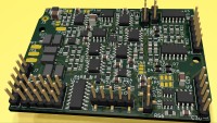
A screenshot of the PCB and the BOM of the C meter are attached also. Please note that the shown version of the C meter has not been tested yet; three PCBs have been ordered and shall arrive before end of November.
Please excuse inconsistencies in the annotation of the components in different schematics.
Please feel free to ask for more details!
I will keep you informed about the progress of the project.
I would like to encourage you to make comments (e.g. proposals for improvements) on the project!
Please note that there are still several open questions reagarding the project, e.g.:
- Which types of test fixtures should be used for different types of DUT (SMD and THT)?
- How high should the accuracy be (and how much are the users willing to pay for it)?
- Is there any interest in selecting capacitors (e.g. a test fixture for say 10 DUTs and a display of the best 2, 3, or 4 matches)
- Optimization of the layout of the PCB (currently having 4 layers), e.g. regarding power planes
- Simplification of the design (without reducing accuracy), e.g. less power supplies
- Your question!
Want to build a project?
Bring your design to life with the Elektor PCB Service, powered by Eurocircuits. Upload the project files and order professionally manufactured PCBs or assembled boards through a proven European production platform.
Supporting KiCad, Eagle, Gerber, and ODB++ formats, the service is suitable for everything from prototypes and validation builds to series production and volume manufacturing.
Made in Europe. Fast. Reliable. Professional.
Mises à jour de l'auteur